Samsung SGH-C240 service manual.pdf
Samsung SGH-C240 service manual.pdf
Samsung SGH-C240 service manual.pdf

You also want an ePaper? Increase the reach of your titles
YUMPU automatically turns print PDFs into web optimized ePapers that Google loves.
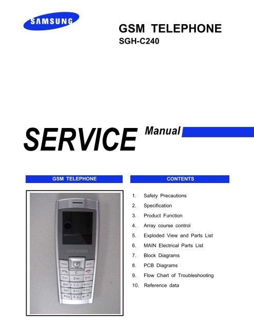
GSM TELEPHONE<br />
<strong>SGH</strong>-<strong>C240</strong><br />
GSM TELEPHONE CONTENTS<br />
1. Safety Precautions<br />
2. Specification<br />
3. Product Function<br />
4. Array course control<br />
5. Exploded View and Parts List<br />
6. MAIN Electrical Parts List<br />
7. Block Diagrams<br />
8. PCB Diagrams<br />
9. Flow Chart of Troubleshooting<br />
10. Reference data
1. Safety Precautions<br />
CONTENTS<br />
1-1. Repair Precaution......................................................................................................1-1<br />
1-2. ESD(Electrostatically Sensitive Devices) Precaution...............................................1-2<br />
2. Specification<br />
2-1. GSM General Specification.......................................................................................2-1<br />
2-2. GSM Tx Power Class...............................................................................................2-2<br />
3. Product Function<br />
4. Array course control<br />
4-1. Software Adjustments................................................................................................4-1<br />
4-2. Software Downloading...............................................................................................4-2<br />
5. Exploded View/Disassembly & Assembly Instructions<br />
5-1. Cellular phone Exploded View..................................................................................5-1<br />
5-2. Cellular phone Part list.............................................................................................5-2<br />
5-3. Disassembly & Assembly Instructions......................................................................5-4<br />
6. MAIN Electrical Parts List<br />
7. Block Diagrams<br />
8. PCB Diagrams
9. Flow Chart of Troubleshooting<br />
CONTENTS<br />
9-1. Baseband<br />
9-1-1. Power On................................................................................................................9-1<br />
9-1-2. Initial........................................................................................................................9-3<br />
9-1-3. Sim Part..................................................................................................................9-5<br />
9-1-4. Microphone Part......................................................................................................9-7<br />
9-1-5. Speaker Part...........................................................................................................9-9<br />
9-1-6. LCD Backlight.......................................................................................................9-11<br />
9-2. RF<br />
9-2-1. GSM RX................................................................................................................9-12<br />
9-2-2. DCS RX................................................................................................................9-14<br />
9-2-3. GSM TX................................................................................................................9-17<br />
9-2-4. DCS Tx.................................................................................................................9-19<br />
10. Reference data
1. Safety Precautions<br />
1-1. Repair Precaution<br />
● Repair in Shield Box, during detailed tuning.<br />
Take specially care of tuning or test,<br />
because specipicty of cellular phone is sensitive for surrounding interference(RF noise).<br />
● Be careful to use a kind of magnetic object or tool,<br />
because performance of parts is damaged by the influence of manetic force.<br />
● Surely use a standard screwdriver when you disassemble this product,<br />
otherwise screw will be worn away.<br />
● Use a thicken twisted wire when you measure level.<br />
A thicken twisted wire has low resistance, therefore error of measurement is few.<br />
● Repair after separate Test Pack and Set because for short danger (for example an<br />
overcurrent and furious flames of parts etc) when you repair board in condition of<br />
connecting Test Pack and tuning on.<br />
● Take specially care of soldering, because Land of PCB is small and weak in heat.<br />
● Surely tune on/off while using AC power plug, because a repair of battery charger is<br />
dangerous when tuning ON/OFF PBA and Connector after disassembing charger.<br />
● Don't use as you pleases after change other material than replacement registered on SEC<br />
System. Otherwise engineer in charge isn't charged with problem that you don't keep this<br />
rules.<br />
1-1<br />
SAMSUNG Proprietary-Contents may change without notice<br />
This Document can not be used without <strong>Samsung</strong>'s authorization
Safety Precautions<br />
1-2. ESD(Electrostatically Sensitive Devices) Precaution<br />
Several semiconductor may be damaged easilly by static electricity. Such parts are called by<br />
ESD(Electrostatically Sensitive Devices), for example IC,BGA chip etc. Read Precaution below.<br />
You can prevent from ESD damage by static electricity.<br />
● Remove static electricity remained your body before you touch semiconductor or parts with<br />
semiconductor. There are ways that you touch an earthed place or wear static electricity<br />
prevention string on wrist.<br />
● Use earthed soldering steel when you connect or disconnect ESD.<br />
● Use soldering removing tool to break static electricity. , otherwise ESD will be damaged by<br />
static electricity.<br />
● Don't unpack until you set up ESD on product. Because most of ESD are packed by box<br />
and aluminum plate to have conductive power,they are prevented from static electricity.<br />
● You must maintain electric contact between ESD and place due to be set up until ESD is<br />
connected completely to the proper place or a circuit board.<br />
1-2<br />
SAMSUNG Proprietary-Contents may change without notice<br />
This Document can not be used without <strong>Samsung</strong>'s authorization
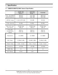
2. Specification<br />
2-1. GSM General Specification<br />
Freq. Band[MHz]<br />
Uplink/Downlink<br />
GSM900<br />
Phase 1<br />
890~915<br />
935~960<br />
2-1<br />
EGSM 900<br />
Phase 2<br />
880~915<br />
925~960<br />
DCS1800<br />
Phase 1<br />
1710~1785<br />
1805~1880<br />
ARFCN range 1~124 0~124 & 975~1023 512~885<br />
Tx/Rx spacing 45MHz 45MHz 95MHz<br />
Mod. Bit rate/<br />
Bit Period<br />
Time Slot Period/Frame<br />
Period<br />
270.833kbps<br />
3.692us<br />
576.9us<br />
4.615ms<br />
270.833kbps<br />
3.692us<br />
576.9us<br />
4.615ms<br />
270.833kbps<br />
3.692us<br />
576.9us<br />
4.615ms<br />
Modulation 0.3GMSK 0.3GMSK 0.3GMSK<br />
MS Power 33dBm~13dBm 33dBm~5dBm 30dBm~0dBm<br />
Power Class 5pcl ~ 15pcl 5pcl ~ 19pcl 0pcl ~ 15pcl<br />
Sensitivity -102dBm -102dBm -100dBm<br />
TDMA Mux 8 8 8<br />
Cell Radius 35Km 35Km 2Km
Speclflcation<br />
2-2. GSM Tx Power Class<br />
TX Power<br />
control level<br />
GSM900<br />
2-2<br />
TX Power<br />
control level<br />
DCS1800<br />
5 33±2 dBm 0 30±3 dBm<br />
6 31±2 dBm 1 28±3 dBm<br />
7 29±2 dBm 2 26±3 dBm<br />
8 27±2 dBm 3 24±3 dBm<br />
9 25±2 dBm 4 22±3 dBm<br />
10 23±2 dBm 5 20±3 dBm<br />
11 21±2 dBm 6 18±3 dBm<br />
12 19±2 dBm 7 16±3 dBm<br />
13 17±2 dBm 8 14±3 dBm<br />
14 15±2 dBm 9 12±4 dBm<br />
15 13±2 dBm 10 10±4 dBm<br />
16 11±3 dBm 11 8±4dBm<br />
17 9±3dBm 12 6±4 dBm<br />
18 7±3 dBm 13 4±4 dBm<br />
19 5±3 dBm 14 2±5 dBm<br />
15 0±5 dBm
3. Product Function<br />
Main Function<br />
-Name card<br />
Create name cards with your number and profile. Whenever introducing yourself to<br />
others, use this convenient electronic name card.<br />
-Web browser<br />
Access the wireless web to get current information and up-to-the-minute a wide<br />
variety of media content.<br />
-Multimedia Message Service (MMS)<br />
Send and receive MMS messages with a combination of text, image, video, and<br />
audio.<br />
-E-mail<br />
Send and receive-emails with image, video,and audio attachments.<br />
-Java<br />
Enjoy Java-based embedded games and download new games.<br />
-Calendar<br />
Keep track of your daily, weekly, and monthly schedule.<br />
-Voice recorder<br />
Record memos or sounds.<br />
3-1<br />
SAMSUNG Proprietary-Contents may change without notice<br />
This Document can not be used without <strong>Samsung</strong>'s authorization
Product Function<br />
3-2<br />
SAMSUNG Proprietary-Contents may change without notice<br />
This Document can not be used without <strong>Samsung</strong>'s authorization
4. Array course control<br />
4-1. Software Adjustments<br />
TEST JIG (GH80-00865A)<br />
DATA CABLE<br />
(GH39-00127A)<br />
RF Test Cable<br />
(GH39-00283A)<br />
4-1<br />
SAMSUNG Proprietary-Contents may change without notice<br />
This Document can not be used without <strong>Samsung</strong>'s authorization
Array course control<br />
4-2. Software Downloading<br />
4-2-1. Downloading Binary File<br />
• Binary file for downloading <strong>C240</strong>.<br />
– <strong>C240</strong>XXYY.s3 : Main source code binary.<br />
4-2-2. Pre-requsite for Downloading<br />
• Downloader Program(OptiFlash.exe)<br />
• <strong>C240</strong> Mobile Phone<br />
• Data Cable<br />
• Binary file<br />
4-2-3. S/W Downloader Program<br />
1. Load the binary download program by executing the “OptiFlash.exe”<br />
2. Select the “Options” -> “Settings” -> “Generic” -> “Specify hardware platform”.<br />
Choose hardware platform for the downloader file setting.<br />
4-2<br />
SAMSUNG Proprietary-Contents may change without notice<br />
This Document can not be used without <strong>Samsung</strong>'s authorization
Set the everything else as the default values which are shown below<br />
3. Select the COM port when the download cable is connected<br />
4-3<br />
SAMSUNG Proprietary-Contents may change without notice<br />
This Document can not be used without <strong>Samsung</strong>'s authorization<br />
Array course control
Array course control<br />
Up to twelve ports are supported. Additionally you can select the maximum<br />
transfer speed OptiFlash will use to communicate with the phone. However,<br />
OptiFlash will use a slower speed if either the PC’s or the phone’s serial<br />
hardware is incapable of handling the selected speed<br />
4. Select the“Flash&Verify” -> “Browse”<br />
Set the directory path and choose the latest s/w binary, for example<br />
“<strong>C240</strong>XXYY.s3”,for the downloader binary setting.<br />
Make sure that not to change the reserved memory regions.<br />
In case of <strong>C240</strong> the reserved regions are :<br />
- 0x00c00000 - 0x00c9ffff<br />
4-4<br />
SAMSUNG Proprietary-Contents may change without notice<br />
This Document can not be used without <strong>Samsung</strong>'s authorization
4-5<br />
SAMSUNG Proprietary-Contents may change without notice<br />
This Document can not be used without <strong>Samsung</strong>'s authorization<br />
Array course control<br />
5. Click “OK” button then press “Flash”.<br />
(Before pressing ‘Flash’ button, push the button ‘*’and ‘END’ at the same time. Then<br />
press ‘Flash’.)<br />
Downloader will upload the binary file as below for the downloading.<br />
6. When downloading is finished successfully, there is a “All is well” message.<br />
7. After finishing downloading, Certain memory resets should be done to guarantee the<br />
normal performance.<br />
8. Confirm the downloaded version name and etc. :<br />
*#5002*8376263#<br />
Full Reset :<br />
*2767*3855#
Array course control<br />
4-6<br />
SAMSUNG Proprietary-Contents may change without notice<br />
This Document can not be used without <strong>Samsung</strong>'s authorization
5. Exploded View/Disassembly&Assembly Instructions<br />
5-1. Cellular phone Exploded View<br />
QMW02<br />
QFR01<br />
QAR01<br />
QLC01<br />
QMP01<br />
QAN05<br />
QSP01<br />
QAN02<br />
QSC01<br />
QRE01<br />
QRF01<br />
QRF03<br />
5-1<br />
QIF01<br />
QKP01<br />
QME01<br />
QMI01<br />
QMO01<br />
QCR06<br />
QBA01<br />
QBA00<br />
SAMSUNG Proprietary-Contents may change without notice<br />
This Document can not be used without <strong>Samsung</strong>'s authorization
Exploded View/Disassembly&Assembly Instructions<br />
5-2. Cellular phone Parts List<br />
Design LOC Description SEC CODE<br />
QAN02 INTENNA-<strong>SGH</strong><strong>C240</strong> GH42-00891A<br />
QAN05 ASSY RUBBER-INTENNA CONTACT GH98-03564A<br />
QAR01 AUDIO-RECEIVER 3009-001214<br />
QBA00 PMO-COVER BATTERY V3 GH72-35740A<br />
QBA01 INNER BATTERY PACK-750MAH,BLK, GH43-02483A<br />
QCR06 SCREW-MACHINE 6001-001155<br />
QFR01 ASSY CASE-FRONT GH98-01615A<br />
QKP01 ASSY KEYPAD-(SER/SIL) GH98-01995A<br />
QLC01 LCD-LCD MODULE GH07-00928A<br />
QME01 UNIT-METAL DOME GH59-03278A<br />
QMI01 MICROPHONE-ASSY-<strong>SGH</strong><strong>C240</strong> GH30-00288A<br />
QMO01 MOTOR DC-<strong>SGH</strong><strong>C240</strong> GH31-00268A<br />
QMP01 PBA MAIN-<strong>SGH</strong><strong>C240</strong> GH92-02900A<br />
QMW02 PCT-COVER WINDOW MAIN GH72-34846A<br />
QRF01 MPR-TAPE SHEET RF COVER GH74-27237A<br />
QSC01 MPR-TAPE SHEET INTENNA COVER GH74-27823A<br />
QSP01 SPEAKER 3001-002018<br />
QRE01 ASSY CASE-REAR GH98-01616A<br />
QIF01 PMO-IF COVER V4 GH72-36725A<br />
QRF03 PMO-COVER EAR V4 GH72-35742A<br />
5-2<br />
SAMSUNG Proprietary-Contents may change without notice<br />
This Document can not be used without <strong>Samsung</strong>'s authorization
5-3<br />
Exploded View/Disassembly&Assembly Instructions<br />
Description SEC CODE<br />
BAG PE 6902-000634<br />
ADAPTOR-<strong>SGH</strong>D500 TA GH44-01451A<br />
UNIT-EARPHONE(SIL) GH59-02472B<br />
LABEL(P)-WATER SOAK GH68-02026A<br />
LABEL(P)-WATER SOAK GH68-02026A<br />
MANUAL-SFC GH68-04336A<br />
LABEL(P)-BARCODE RUSSIA GH68-08494A<br />
LABEL(R)-MAIN(SER) GH68-11762C<br />
MANUAL USERS-EU RUSSIAN GH68-11868A<br />
BOX-UNIT(SER) GH69-04190B<br />
MPR-SPONGE INTENNA CARRIER GH74-27236A<br />
MPR-TAPE RECEIVER GH74-29274A<br />
MPR-TAPE EMI SHEET GH74-29420A<br />
SAMSUNG Proprietary-Contents may change without notice<br />
This Document can not be used without <strong>Samsung</strong>'s authorization
Exploded View/Disassembly&Assembly Instructions<br />
5-3. Disassembly&Assembly Instructions<br />
― Disassembly<br />
1 2<br />
1. Loosen a screw this four point form Rear.<br />
2. And remove the IF cover.<br />
3 4<br />
1. Separate the PBA from front cover<br />
regard of 2 hooks and lift up.<br />
5-4<br />
1. Make the space between rear cover and<br />
front cover using assembly stick.<br />
2. And then widen space with hand and<br />
separate 2 parts.<br />
1. Remove the tape from front cover.<br />
2. And Remove the receiver from front cover<br />
using removing hole.<br />
SAMSUNG Proprietary-Contents may change without notice<br />
This Document can not be used without <strong>Samsung</strong>'s authorization
5 6<br />
1. Loosen the 4 hooks of intenna carrier from<br />
PBA board and separate.<br />
7<br />
1. Remove the LCD module from PBA board<br />
using soldering tip.<br />
5-5<br />
Exploded View/Disassembly&Assembly Instructions<br />
1. And separate the LCD module from PBA<br />
board using removing hole with pinset.<br />
1. Verify all kinds of elements after finishing<br />
disassembling<br />
SAMSUNG Proprietary-Contents may change without notice<br />
This Document can not be used without <strong>Samsung</strong>'s authorization<br />
8
Exploded View/Disassembly&Assembly Instructions<br />
― Assembly<br />
1 2<br />
1.RemovethetapecoverandattachtheLCD<br />
FPCB to PBA board using 2 point of mark<br />
2. And soldering the module and attach the<br />
LCD module on PBA regarding guide hole.<br />
3 4<br />
5-6<br />
1. Assemble the intenna carrier to PBA board<br />
using hooks like picture.<br />
1. Insert the receiver to receiver hole and push. 1.InserttheupsideofPBAtofront<br />
2. Attach the Tape on receiver air hole like 2. And locking the hook like picture.<br />
apicture.<br />
3. Insert the mic in mic hole on front.<br />
SAMSUNG Proprietary-Contents may change without notice<br />
This Document can not be used without <strong>Samsung</strong>'s authorization
5 6<br />
5-7<br />
Exploded View/Disassembly&Assembly Instructions<br />
1. Assemble the rear to front from top side. 1. Fasten the 4 point of screw like picture.<br />
SAMSUNG Proprietary-Contents may change without notice<br />
This Document can not be used without <strong>Samsung</strong>'s authorization
Exploded View/Disassembly&Assembly Instructions<br />
5-8<br />
SAMSUNG Proprietary-Contents may change without notice<br />
This Document can not be used without <strong>Samsung</strong>'s authorization
6. Electrical Parts List<br />
Design LOC Description SEC CODE STATUS<br />
ANT100 NPR-ANTENNA CONTACT GH71-04813A SA<br />
ANT101 NPR-ANTENNA CONTACT GH71-04813A SA<br />
BAT200 BATTERY-LI(2ND) 4302-001130 SA<br />
BTC800 HEADER-BATTERY 3711-006084 SA<br />
C101 C-CER,CHIP 2203-000995 SA<br />
C103 C-CER,CHIP 2203-002668 SA<br />
C113 C-CER,CHIP 2203-006048 SA<br />
C114 C-CER,CHIP 2203-000854 SA<br />
C115 C-CER,CHIP 2203-000278 SA<br />
C117 C-CER,CHIP 2203-000233 SA<br />
C123 C-CER,CHIP 2203-006048 SA<br />
C124 C-CER,CHIP 2203-000386 SA<br />
C125 C-CER,CHIP 2203-000812 SA<br />
C126 C-CER,CHIP 2203-006048 SA<br />
C127 C-CER,CHIP 2203-005234 SA<br />
C128 C-CER,CHIP 2203-005234 SA<br />
C129 C-CER,CHIP 2203-001017 SA<br />
C130 C-CER,CHIP 2203-005050 SA<br />
C131 C-CER,CHIP 2203-000278 SA<br />
C132 C-CER,CHIP 2203-005050 SA<br />
C135 C-TA,CHIP 2404-001474 SA<br />
C136 C-CER,CHIP 2203-006048 SA<br />
C137 C-CER,CHIP 2203-006048 SA<br />
C139 C-CER,CHIP 2203-000359 SA<br />
C141 C-CER,CHIP 2203-000585 SA<br />
C142 C-CER,CHIP 2203-006048 SA<br />
C143 C-CER,CHIP 2203-006048 SA<br />
C200 C-CER,CHIP 2203-000254 SA<br />
C201 C-CER,CHIP 2203-001072 SA<br />
C202 C-CER,CHIP 2203-006048 SA<br />
C203 C-CER,CHIP 2203-006324 SA<br />
C204 C-CER,CHIP 2203-000995 SA<br />
C205 C-CER,CHIP 2203-000812 SA<br />
C206 C-CER,CHIP 2203-000812 SA<br />
C207 C-CER,CHIP 2203-002709 SA<br />
C208 C-CER,CHIP 2203-006183 SA<br />
C209 C-CER,CHIP 2203-000233 SA<br />
C210 C-TA,CHIP 2404-001240 SA<br />
C211 C-CER,CHIP 2203-006183 SA<br />
C212 C-CER,CHIP 2203-006562 SA<br />
C213 C-CER,CHIP 2203-006562 SA<br />
C214 C-CER,CHIP 2203-006562 SA<br />
C215 C-CER,CHIP 2203-006562 SA<br />
C216 C-CER,CHIP 2203-006562 SA<br />
C217 C-CER,CHIP 2203-000254 SA<br />
C218 C-CER,CHIP 2203-002709 SA<br />
C219 C-CER,CHIP 2203-000254 SA<br />
C220 C-CER,CHIP 2203-005819 SA<br />
C223 C-CER,CHIP 2203-006348 SA<br />
C224 C-TA,CHIP 2404-001381 SA<br />
C300 C-CER,CHIP 2203-000254 SA<br />
C301 C-CER,CHIP 2203-000254 SA<br />
C302 C-CER,CHIP 2203-000254 SA<br />
C303 C-CER,CHIP 2203-000254 SA<br />
C304 C-CER,CHIP 2203-006260 SA<br />
6-1<br />
SAMSUNG Proprietary-Contents may change without notice<br />
This Document can not be used without <strong>Samsung</strong>'s authorization
Electrical Parts List<br />
Design LOC Description SEC CODE STATUS<br />
C305 C-CER,CHIP 2203-002709 SA<br />
C306 C-CER,CHIP 2203-000679 SA<br />
C307 C-CER,CHIP 2203-000254 SA<br />
C308 C-CER,CHIP 2203-002709 SA<br />
C309 C-CER,CHIP 2203-000254 SA<br />
C310 C-CER,CHIP 2203-000254 SA<br />
C311 C-CER,CHIP 2203-000254 SA<br />
C312 C-CER,CHIP 2203-000254 SA<br />
C313 C-CER,CHIP 2203-006260 SA<br />
C315 C-CER,CHIP 2203-000330 SA<br />
C316 C-CER,CHIP 2203-000330 SA<br />
C317 C-CER,CHIP 2203-006626 SA<br />
C400 C-CER,CHIP 2203-000330 SA<br />
C402 C-CER,CHIP 2203-006260 SA<br />
C404 C-CER,CHIP 2203-000995 SA<br />
C407 C-CER,CHIP 2203-006260 SA<br />
C408 C-CER,CHIP 2203-001153 SA<br />
C410 C-TA,CHIP 2404-001414 SA<br />
C411 C-CER,CHIP 2203-000233 SA<br />
C412 C-CER,CHIP 2203-006048 SA<br />
C413 C-CER,CHIP 2203-000330 SA<br />
C416 C-CER,CHIP 2203-000995 SA<br />
C417 C-CER,CHIP 2203-000278 SA<br />
C418 C-CER,CHIP 2203-006048 SA<br />
C419 C-CER,CHIP 2203-001153 SA<br />
C420 C-CER,CHIP 2203-001153 SA<br />
C422 C-CER,CHIP 2203-000254 SA<br />
C423 C-CER,CHIP 2203-001405 SA<br />
C500 C-CER,CHIP 2203-006466 SA<br />
C503 C-CER,CHIP 2203-000940 SA<br />
C504 C-TA,CHIP 2404-001381 SA<br />
C505 C-CER,CHIP 2203-002709 SA<br />
C506 C-CER,CHIP 2203-006091 SA<br />
C507 C-CER,CHIP 2203-006825 SA<br />
C508 C-CER,CHIP 2203-006165 SA<br />
C509 C-CER,CHIP 2203-005061 SA<br />
C511 C-CER,CHIP 2203-001072 SA<br />
C512 C-CER,CHIP 2203-001072 SA<br />
C513 C-CER,CHIP 2203-000585 SA<br />
C514 C-CER,CHIP 2203-002709 SA<br />
C515 C-CER,CHIP 2203-006260 SA<br />
C516 C-CER,CHIP 2203-000438 SA<br />
C517 C-CER,CHIP 2203-006824 SA<br />
C518 C-CER,CHIP 2203-002709 SA<br />
C519 C-TA,CHIP 2404-001240 SA<br />
C520 C-CER,CHIP 2203-006048 SA<br />
C521 C-CER,CHIP 2203-005482 SA<br />
C522 C-CER,CHIP 2203-006635 SA<br />
C523 C-CER,CHIP 2203-005993 SA<br />
C524 C-CER,CHIP 2203-006260 SA<br />
C525 C-CER,CHIP 2203-005481 SA<br />
C528 C-CER,CHIP 2203-005481 SA<br />
C529 C-CER,CHIP 2203-006260 SA<br />
C532 C-CER,CHIP 2203-005482 SA<br />
C534 C-CER,CHIP 2203-000995 SA<br />
6-2<br />
SAMSUNG Proprietary-Contents may change without notice<br />
This Document can not be used without <strong>Samsung</strong>'s authorization
6-3<br />
SAMSUNG Proprietary-Contents may change without notice<br />
This Document can not be used without <strong>Samsung</strong>'s authorization<br />
Electrical Parts List<br />
Design LOC Description SEC CODE STATUS<br />
C535 C-CER,CHIP 2203-006324 SA<br />
C537 C-CER,CHIP 2203-000679 SA<br />
C538 C-CER,CHIP 2203-000359 SA<br />
C601 C-CER,CHIP 2203-000233 SA<br />
C602 C-CER,CHIP 2203-002709 SA<br />
C603 C-CER,CHIP 2203-000233 SA<br />
C604 C-CER,CHIP 2203-002709 SA<br />
C605 C-CER,CHIP 2203-000254 SA<br />
C700 C-CER,CHIP 2203-006324 SA<br />
C701 C-TA,CHIP 2404-001450 SA<br />
C702 C-CER,CHIP 2203-006562 SA<br />
C800 C-NETWORK 2503-001053 SA<br />
C801 C-NETWORK 2503-001053 SA<br />
C802 C-NETWORK 2503-001053 SA<br />
C803 C-CER,CHIP 2203-000438 SA<br />
C804 C-TA,CHIP 2404-001381 SA<br />
C805 C-CER,CHIP 2203-000854 SA<br />
CON100 CONNECTOR-COAXIAL 3705-001358 SA<br />
D500 DIODE-ARRAY 0407-001002 SA<br />
D501 DIODE-TVS 0406-001223 SA<br />
D502 DIODE-TVS 0406-001223 SA<br />
D503 DIODE-TVS 0406-001223 SA<br />
D504 DIODE-TVS 0406-001223 SA<br />
EAR400 JACK-EAR PHONE 3722-002010 SA<br />
F100 DUPLEXER-ASM 2911-000067 SA<br />
F101 FILTER-SAW 2904-001744 SA<br />
F800 FILTER-EMI SMD 2901-001254 SA<br />
IFC800 CONNECTOR-INTERFACE 3710-001611 SA<br />
L102 R-CHIP 2007-000171 SA<br />
L103 INDUCTOR-SMD 2703-002269 SA<br />
L105 C-CER,CHIP 2203-000550 SA<br />
L106 C-CER,CHIP 2203-000995 SA<br />
L107 INDUCTOR-SMD 2703-002370 SA<br />
L108 INDUCTOR-SMD 2703-002170 SA<br />
L109 INDUCTOR-SMD 2703-001990 SA<br />
L110 INDUCTOR-SMD 2703-002199 SA<br />
L400 INDUCTOR-SMD 2703-002202 SA<br />
L401 INDUCTOR-SMD 2703-002202 SA<br />
L402 BEAD-SMD 3301-001729 SA<br />
L403 BEAD-SMD 3301-001729 SA<br />
L404 BEAD-SMD 3301-001729 SA<br />
L405 BEAD-SMD 3301-001729 SA<br />
L406 BEAD-SMD 3301-001729 SA<br />
L407 INDUCTOR-SMD 2703-001231 SNA<br />
L408 BEAD-SMD 3301-001729 SA<br />
L501 INDUCTOR-SMD 2703-001180 SA<br />
L502 INDUCTOR-SMD 2703-002206 SA<br />
L503 INDUCTOR-SMD 2703-001180 SA<br />
L504 INDUCTOR-SMD 2703-001673 SA<br />
L700 INDUCTOR-SMD 2703-002768 SNA<br />
L800 BEAD-SMD 3301-001659 SA<br />
LED700 LED 0601-002037 SA<br />
LED701 LED 0601-002037 SA<br />
LED702 LED 0601-002037 SA<br />
LED703 LED 0601-002037 SA
Electrical Parts List<br />
Design LOC Description SEC CODE STATUS<br />
LED704 LED 0601-002037 SA<br />
LED705 LED 0601-002037 SA<br />
LED706 LED 0601-002037 SA<br />
LED707 LED 0601-002037 SA<br />
LED708 LED 0601-002037 SA<br />
LED709 LED 0601-002037 SA<br />
LED710 LED 0601-002037 SA<br />
MEM600 IC-MCP 1108-000010 SA<br />
OSC100 CRYSTAL-SMD 2801-004426 SA<br />
OSC300 CRYSTAL-SMD 2801-003856 SA<br />
PAM100 IC-POWER AMP 1201-002425 SA<br />
R100 R-CHIP 2007-001298 SA<br />
R101 R-CHIP 2007-002970 SA<br />
R104 R-CHIP 2007-000171 SA<br />
R105 R-CHIP 2007-002797 SA<br />
R106 R-CHIP 2007-000148 SA<br />
R107 R-CHIP 2007-001308 SA<br />
R108 R-CHIP 2007-000171 SA<br />
R111 R-CHIP 2007-000147 SA<br />
R200 R-CHIP 2007-000144 SA<br />
R201 R-CHIP 2007-000171 SA<br />
R203 R-CHIP 2007-000171 SA<br />
R208 R-CHIP 2007-000171 SA<br />
R209 R-CHIP 2007-000167 SA<br />
R210 R-CHIP 2007-000172 SA<br />
R212 R-CHIP 2007-000172 SA<br />
R213 R-CHIP 2007-000162 SA<br />
R215 R-CHIP 2007-007142 SA<br />
R216 R-CHIP 2007-000154 SA<br />
R217 R-CHIP 2007-000153 SA<br />
R218 R-CHIP 2007-000162 SA<br />
R219 R-CHIP 2007-000140 SA<br />
R220 R-CHIP 2007-000171 SA<br />
R300 R-CHIP 2007-000157 SA<br />
R301 R-CHIP 2007-000157 SA<br />
R302 R-CHIP 2007-000162 SA<br />
R303 R-CHIP 2007-000171 SA<br />
R304 R-CHIP 2007-007480 SA<br />
R305 R-CHIP 2007-000157 SA<br />
R306 R-CHIP 2007-000159 SA<br />
R307 R-CHIP 2007-007142 SA<br />
R308 R-CHIP 2007-000171 SA<br />
R309 R-CHIP 2007-007573 SA<br />
R310 R-CHIP 2007-000162 SA<br />
R311 R-CHIP 2007-007573 SA<br />
R312 R-CHIP 2007-000143 SA<br />
R313 R-CHIP 2007-000143 SA<br />
R315 R-CHIP 2007-000171 SA<br />
R400 R-CHIP 2007-007107 SA<br />
R401 R-CHIP 2007-007142 SA<br />
R403 R-CHIP 2007-007142 SA<br />
R404 R-CHIP 2007-007107 SA<br />
R405 R-CHIP 2007-001320 SA<br />
R406 R-CHIP 2007-000142 SA<br />
R407 R-CHIP 2007-001317 SA<br />
6-4<br />
SAMSUNG Proprietary-Contents may change without notice<br />
This Document can not be used without <strong>Samsung</strong>'s authorization
6-5<br />
SAMSUNG Proprietary-Contents may change without notice<br />
This Document can not be used without <strong>Samsung</strong>'s authorization<br />
Electrical Parts List<br />
Design LOC Description SEC CODE STATUS<br />
R409 R-CHIP 2007-001320 SA<br />
R410 R-CHIP 2007-000142 SA<br />
R411 R-CHIP 2007-007142 SA<br />
R412 R-CHIP 2007-007101 SA<br />
R413 R-CHIP 2007-007101 SA<br />
R414 R-CHIP 2007-007142 SA<br />
R415 R-CHIP 2007-007573 SA<br />
R416 R-CHIP 2007-007480 SA<br />
R417 R-CHIP 2007-001339 SA<br />
R418 R-CHIP 2007-000162 SA<br />
R419 R-CHIP 2007-001317 SA<br />
R420 R-CHIP 2007-000172 SA<br />
R421 R-CHIP 2007-000172 SA<br />
R422 R-CHIP 2007-000171 SA<br />
R500 R-CHIP 2007-007156 SA<br />
R501 R-CHIP 2007-007156 SA<br />
R502 R-CHIP 2007-000171 SA<br />
R503 R-CHIP 2007-000162 SA<br />
R504 R-CHIP 2007-007021 SA<br />
R505 R-CHIP 2007-001329 SA<br />
R506 R-CHIP 2007-000172 SA<br />
R507 R-CHIP 2007-000172 SA<br />
R508 R-CHIP 2007-001325 SA<br />
R509 R-CHIP 2007-003001 SA<br />
R510 R-CHIP 2007-000171 SA<br />
R511 R-CHIP 2007-008137 SA<br />
R512 R-CHIP 2007-008137 SA<br />
R513 R-CHIP 2007-000162 SA<br />
R514 R-CHIP 2007-000171 SA<br />
R515 R-CHIP 2007-000172 SA<br />
R516 R-CHIP 2007-000172 SA<br />
R601 R-CHIP 2007-000172 SA<br />
R602 R-CHIP 2007-000171 SA<br />
R700 R-CHIP 2007-001307 SA<br />
R701 R-CHIP 2007-001301 SA<br />
R702 R-CHIP 2007-001308 SA<br />
R703 R-CHIP 2007-003004 SA<br />
R704 R-CHIP 2007-003004 SA<br />
R705 R-CHIP 2007-001307 SA<br />
R706 R-CHIP 2007-001307 SA<br />
R707 R-CHIP 2007-002970 SA<br />
R708 R-CHIP 2007-003030 SA<br />
R709 R-CHIP 2007-001307 SA<br />
R710 R-CHIP 2007-003030 SA<br />
R711 R-CHIP 2007-000171 SA<br />
R712 R-CHIP 2007-003001 SA<br />
R800 R-CHIP 2007-000171 SA<br />
R801 R-CHIP 2007-000171 SA<br />
R802 R-CHIP 2007-000171 SA<br />
R803 R-CHIP 2007-000566 SA<br />
R804 R-CHIP 2007-000566 SA<br />
R805 R-CHIP 2007-000566 SA<br />
R806 R-CHIP 2007-000566 SA<br />
R807 R-CHIP 2007-000566 SA<br />
R808 R-CHIP 2007-000140 SA
Electrical Parts List<br />
Design LOC Description SEC CODE STATUS<br />
R809 R-CHIP 2007-000140 SA<br />
R810 R-CHIP 2007-000140 SA<br />
R811 R-CHIP 2007-000140 SA<br />
R812 R-CHIP 2007-000140 SA<br />
R813 R-CHIP 2007-000140 SA<br />
R814 R-CHIP 2007-000140 SA<br />
R815 R-CHIP 2007-000140 SA<br />
R816 R-CHIP 2007-000140 SA<br />
R817 R-CHIP 2007-000140 SA<br />
R818 R-CHIP 2007-000171 SA<br />
R819 R-CHIP 2007-000140 SA<br />
R820 R-CHIP 2007-000140 SA<br />
SIM200 CONNECTOR-CARD EDGE 3709-001229 SA<br />
TH300 THERMISTOR-NTC 1404-001221 SA<br />
TR200 TR-DIGITAL 0504-000168 SA<br />
U101 IC-TRANSCEIVER 1205-003116 SA<br />
U201 IC-BATTERY 1203-003663 SA<br />
U202 IC-CMOS LOGIC 0801-000796 SA<br />
U401 IC-VOLTAGE COMP. 1202-001068 SA<br />
U500 IC-MELODY 1204-001811 SA<br />
U501 IC-DEMODULATOR 1204-002688 SA<br />
U502 IC-AUDIO AMP 1201-002356 SA<br />
U503 IC-POSI.FIXED REG. 1203-003737 SA<br />
U700 VARISTOR 1405-001082 SA<br />
U701 IC-DC/DC CONVERTER 1203-004247 SA<br />
UCP200 IC-POWER SUPERVISOR 1203-003304 SA<br />
UCP300 IC MICOM-<strong>SGH</strong>X480 GH09-00036A SA<br />
VR401 VARISTOR 1405-001082 SA<br />
VR402 VARISTOR 1405-001082 SA<br />
VR403 DIODE-TVS 0406-001223 SA<br />
VR404 DIODE-TVS 0406-001223 SA<br />
VR700 VARISTOR 1405-001082 SA<br />
VR701 DIODE-TVS 0406-001223 SA<br />
VR702 DIODE-TVS 0406-001223 SA<br />
VR703 DIODE-TVS 0406-001223 SA<br />
VR704 DIODE-TVS 0406-001223 SA<br />
VR705 DIODE-TVS 0406-001223 SA<br />
VR706 DIODE-TVS 0406-001223 SA<br />
VR707 DIODE-TVS 0406-001223 SA<br />
VR708 DIODE-TVS 0406-001223 SA<br />
VR709 DIODE-TVS 0406-001223 SA<br />
VR710 DIODE-TVS 0406-001223 SA<br />
VR711 DIODE-TVS 0406-001223 SA<br />
VR712 DIODE-TVS 0406-001223 SA<br />
ZD400 DIODE-TVS 0406-001104 SA<br />
ZD800 DIODE-ZENER 0403-001547 SA<br />
ZD801 DIODE-ZENER 0403-001547 SA<br />
ZD802 DIODE-TVS 0406-001190 SA<br />
ZD803 DIODE-TVS 0406-001190 SA<br />
ZD804 DIODE-TVS 0406-001190 SA<br />
6-6<br />
SAMSUNG Proprietary-Contents may change without notice<br />
This Document can not be used without <strong>Samsung</strong>'s authorization
7. Block Diagrams<br />
Antenna<br />
DUAL ASM<br />
(GSM, DCS)<br />
EGSM Rx<br />
DCS Rx<br />
EGSM Tx<br />
DCS Tx<br />
DUAL<br />
SAW FILTER<br />
(GSM, DCS)<br />
PAM<br />
LNA<br />
LNA<br />
LNA<br />
LNA<br />
0 / 90<br />
VCO + FREQUENCY<br />
SYNTHESIZER<br />
7-1<br />
PGA<br />
PGA<br />
ф<br />
DET<br />
I<br />
ADC<br />
Q<br />
ADC<br />
Low-IF<br />
SAMSUNG Proprietary-Contents may change without notice<br />
This Document can not be used without <strong>Samsung</strong>'s authorization<br />
DIGITAL<br />
FILTER<br />
Digital<br />
PGA<br />
PGA<br />
DCXO<br />
Crystal<br />
Si4210<br />
ANALOG INTERFACE<br />
I<br />
Q<br />
XOUT<br />
AFC<br />
CPS2200B1
8. PCB Diagrams<br />
Top<br />
8-1<br />
SAMSUNG Proprietary-Contents may change without notice<br />
This Document can not be used without <strong>Samsung</strong>'s authorization
PCB Diagrams<br />
Bottom<br />
8-2<br />
SAMSUNG Proprietary-Contents may change without notice<br />
This Document can not be used without <strong>Samsung</strong>'s authorization
9. Flow Chart of Troubleshooting<br />
9-1. Baseband<br />
9-1-1. Power ON<br />
'Power ON' does not work<br />
check the current<br />
consumption<br />
>= 100mA<br />
END<br />
Yes<br />
Check the Voltage<br />
of the Battery<br />
>= 3.3V<br />
Yes<br />
Check the pin C152,<br />
C153,C155,C168 of<br />
U107 is<br />
>=2.8V<br />
Yes<br />
Check the clock signal at<br />
pin #4 of OSC100<br />
Freq=26Mhz,<br />
Vrms >=300mV<br />
Yes<br />
Check the Initial Operation<br />
Yes<br />
No<br />
No<br />
No<br />
9-1<br />
Download again<br />
Charge the battery<br />
Check<br />
"Power On"<br />
key?<br />
No<br />
No Check the clock generation<br />
circuit OSC100<br />
check keypad<br />
Yes 1<br />
check UCP200 and C200<br />
2
Flow Chart of Troubleshooting<br />
VCCD VCCA<br />
2<br />
C201<br />
GNDS6<br />
GNDS5 G7<br />
GNDS4 F10<br />
GNDS3 F9<br />
GNDS2 F8<br />
G8<br />
GNDS11<br />
GNDS10 H7<br />
GNDS9 H6<br />
GNDS8 G10<br />
GNDS7 G9<br />
GNDS1 F7<br />
H8<br />
AUX_ADC3 D13<br />
1<br />
VDDB A6<br />
VDDD<br />
VSS4 P6<br />
VSS3 R2<br />
VSS2 K4<br />
VSS1 G5<br />
N11<br />
GND_OCTL B4<br />
VDD_OCTL C4<br />
GNDV P13<br />
VDDV L11<br />
GNDB F6<br />
GNDD M10<br />
VDD_IO2 J4<br />
VDD_IO1 N5<br />
VDD3 N6<br />
M3<br />
9-2<br />
C200
9-1-2. Initial<br />
Initial Failure<br />
check the pin<br />
RSTB of UCP300<br />
is LOW?<br />
END<br />
Yes<br />
check the pin CKI<br />
of UCP300 is<br />
13Mhz?<br />
Yes<br />
Check the clock signal<br />
at pin #3 of OSC100<br />
Freq=26Mhz?<br />
Yes<br />
Check the pin #9 of<br />
UCP300 is HIGH and pin<br />
#11, #13 is 2.9V?<br />
Yes<br />
Check the Initial Operation<br />
Yes<br />
9-3<br />
No<br />
No<br />
No<br />
No<br />
Flow Chart of Troubleshooting<br />
Check UCP300<br />
Check<br />
R104,R108,R200,C124<br />
check OSC100<br />
Check UCP200<br />
1<br />
2<br />
3<br />
4
Flow Chart of Troubleshooting<br />
1<br />
9-4<br />
4<br />
2<br />
3
9-1-3. Sim Part<br />
"Insert SIM" is displayed on the LCD<br />
The voltage is 2.8V<br />
at the pin#1 of<br />
Is there any signal<br />
pin #2,3,4 of<br />
SIM200?<br />
END<br />
Yes<br />
Yes<br />
Check the SIM Card<br />
9-5<br />
No<br />
No<br />
Check the UCP200<br />
Flow Chart of Troubleshooting<br />
Check the UCP200 & UCP300<br />
1<br />
2
Flow Chart of Troubleshooting<br />
2<br />
9-6<br />
1 2
9-1-4.Microphone Part<br />
* Call with Sim before testing.<br />
MicroPhone does not work<br />
Check the soldered<br />
status of microphone<br />
END<br />
Yes<br />
Yes<br />
Check the reference<br />
voltage on mic path<br />
C410 ≒ 2.0V<br />
Yes<br />
Is microphone OK?<br />
Yes<br />
9-7<br />
No<br />
No<br />
No<br />
Resolder microphone<br />
Flow Chart of Troubleshooting<br />
Resolder or change<br />
Check UCP200<br />
2<br />
1
Flow Chart of Troubleshooting<br />
2<br />
9-8<br />
1
9-1-5. Speaker Part<br />
There is no sound from speaker<br />
Are there any signal at<br />
the speaker pad on PCB?<br />
END<br />
No<br />
Check R515, R516 of<br />
U502. Voltage is ≥1V?<br />
Yes<br />
9-9<br />
Yes<br />
No<br />
Flow Chart of Troubleshooting<br />
Replace the speaker module<br />
Check MEM600<br />
1
Flow Chart of Troubleshooting<br />
1<br />
9-10
9-1-6. LCD Backlight<br />
Backlight does not work<br />
Backlight ON "TIME"<br />
mode in the menu?<br />
Check soldering pad<br />
between PBA and LCD<br />
END<br />
Yes<br />
Yes<br />
Check U704 pin #6 =<br />
10V ?<br />
Yes<br />
9-11<br />
No<br />
No<br />
No<br />
Flow Chart of Troubleshooting<br />
Select backlight "15 sec" mode<br />
Check FPCB<br />
Check the LCD
Flow Chart of Troubleshooting<br />
9-2. RF<br />
9-2-1. GSM Rx<br />
CONTINOUS RX ON<br />
RF INPUT : 62CH<br />
AMP : -50dbm<br />
Normal condition<br />
catch the<br />
channel ?<br />
Yes<br />
Check PAM100<br />
pin 12 ≥ -65<br />
dbm ?<br />
Yes<br />
Check PAM100<br />
pin 16 ≥ -65<br />
dbm ?<br />
Yes<br />
Check U101<br />
pin 21,22 ≥-<br />
65dBm ?<br />
Yes<br />
Check U101<br />
pin 13 = 2.9V<br />
Yes<br />
Resolder or change<br />
UCP300<br />
No<br />
No<br />
No<br />
No<br />
No<br />
9-12<br />
Check ANT, R111,R100,C131,L110<br />
Resolder or change<br />
CON100, L103, C100, L102, C101, L104<br />
Resolder or change<br />
PAM100<br />
Resolder or change<br />
F100, F101<br />
Resolder or change<br />
UCP200<br />
1<br />
2<br />
3<br />
4<br />
5
4<br />
5<br />
9-13<br />
4<br />
3<br />
Flow Chart of Troubleshooting<br />
2<br />
1
Flow Chart of Troubleshooting<br />
9-2-2. DCS Rx<br />
CONTINOUS RX ON<br />
RF INPUT : 698CH<br />
AMP : -50dbm<br />
Normal condition<br />
catch the<br />
channel ?<br />
Yes<br />
Check PAM100<br />
pin 12 ≥ -65<br />
dbm ?<br />
Yes<br />
Check PAM100<br />
pin 18 ≥ -65<br />
dbm ?<br />
Yes<br />
Check U101<br />
pin 19,20 ≥-<br />
65dBm ?<br />
Yes<br />
Check U101<br />
pin 13 = 2.9V<br />
Yes<br />
Resolder or change<br />
U300<br />
No<br />
No<br />
No<br />
No<br />
No<br />
9-14<br />
Check ANT,R111,R101,C129,L108<br />
Resolder or change<br />
CON100, L103, C100, L102, C101, L104<br />
Resolder or change<br />
PAM100<br />
Resolder or change<br />
F100, F101<br />
Resolder or change<br />
UCP200<br />
1<br />
2<br />
3<br />
4<br />
5
4<br />
5<br />
9-15<br />
4<br />
1<br />
3<br />
Flow Chart of Troubleshooting<br />
2
Flow Chart of Troubleshooting<br />
9-16
9-2-3. GSM Tx<br />
1<br />
Check U101<br />
pin 15 : about<br />
2~3 dbm?<br />
Yes<br />
Check and<br />
change<br />
CON100,<br />
L105,C103<br />
No<br />
No<br />
PAM100 pin 15<br />
: 3.7V ?<br />
Yes<br />
PAM100 pin 14 :<br />
1.2V ?<br />
Yes<br />
PAM100 pin 5<br />
:about -5dbm?<br />
Yes<br />
PAM100 pin 3<br />
: 3V ?<br />
Yes<br />
PAM100<br />
change or resolder<br />
Check U101<br />
pin 6 : 2.8V ?<br />
Yes<br />
PAM100 pin 5 :<br />
about 4~5dbm?<br />
Yes<br />
U101<br />
check & change<br />
9-17<br />
No<br />
No Battery, UCP200<br />
check & change<br />
No UCP200 check<br />
No<br />
3<br />
No UCP200<br />
check<br />
6<br />
2<br />
Check and<br />
change<br />
UCP300,<br />
UCP200<br />
5<br />
4<br />
U101 pin 12,13,<br />
28,29 : 2.9V ?<br />
Yes<br />
U101<br />
change or resolder<br />
7<br />
Flow Chart of Troubleshooting<br />
CONTINUS TX ON CONDITION<br />
TX POWER DAC : 554 CODE<br />
APPLIED<br />
CH : 62ch<br />
RBW : 100KHz<br />
VBW : 100KHz<br />
SPAN : 10MHz<br />
REF LEV : 10dBm<br />
ATT : 20dB<br />
No<br />
8<br />
UCP200<br />
change or resolder
Flow Chart of Troubleshooting<br />
1<br />
2<br />
2<br />
3<br />
9-18
9-2-4. DCS Tx<br />
1<br />
Check U101<br />
pin 15 : about<br />
2~3 dbm?<br />
Yes<br />
Check and<br />
change<br />
CON100,<br />
L106,L108<br />
No Check U101<br />
pin 6 : 2.8V ?<br />
No<br />
No<br />
PAM100 pin 15<br />
: 3.7V ?<br />
Yes<br />
PAM100 pin 14<br />
: 1.2V ?<br />
Yes<br />
PAM100 pin 9<br />
:about -5dbm?<br />
Yes<br />
PAM100 pin 3<br />
: 3V ?<br />
Yes<br />
PAM100<br />
change or resolder<br />
Yes<br />
PAM100 pin 9<br />
:about 4~5dbm?<br />
Yes<br />
U101<br />
check & change<br />
No<br />
No<br />
No<br />
No<br />
3<br />
9-19<br />
2<br />
Battery, UCP200<br />
check & change<br />
UCP200 check<br />
UCP200<br />
check<br />
6<br />
Check and<br />
change<br />
UCP300,<br />
UCP200<br />
5<br />
4<br />
U101 pin 12,13,<br />
28,29 : 2.9V ?<br />
Yes<br />
U101<br />
change or resolder<br />
7<br />
Flow Chart of Troubleshooting<br />
CONTINUS TX ON CONDITION<br />
TX POWER DAC : 560 CODE<br />
APPLIED<br />
CH : 698CH(DCS),<br />
660CH(PCS)<br />
RBW : 100KHz<br />
VBW : 100KHz<br />
SPAN : 10MHz<br />
REF LEV : 10dBm<br />
ATT : 20dB<br />
No<br />
8<br />
UCP200<br />
change or resolder
Flow Chart of Troubleshooting<br />
1<br />
2<br />
2<br />
3<br />
9-20
10. Reference data<br />
Reference Abbreviate<br />
― AAC: Advanced Audio Coding.<br />
― AVC : Advanced Video Coding.<br />
― BER : Bit Error Rate<br />
― BPSK: Binary Phase Shift Keying<br />
― CA : Conditional Access<br />
― CDM : Code Division Multiplexing<br />
― C/I : Carrier to Interference<br />
― DMB : Digital Multimedia Broadcasting<br />
― EN : European Standard<br />
― ES : Elementary Stream<br />
― ETSI: European Telecommunications Standards Institute<br />
― MPEG: Moving Picture Experts Group<br />
― PN : Pseudo-random Noise<br />
― PS : Pilot Symbol<br />
― QPSK: Quadrature Phase Shift Keying<br />
― RS : Reed-Solomon<br />
― SI : Service Information<br />
― TDM : Time Division Multiplexing<br />
― TS : Transport Stream<br />
10-1<br />
SAMSUNG Proprietary-Contents may change without notice<br />
This Document can not be used without <strong>Samsung</strong>'s authorization
Reference Data<br />
10-2<br />
SAMSUNG Proprietary-Contents may change without notice<br />
This Document can not be used without <strong>Samsung</strong>'s authorization
This Service Manual is a property of <strong>Samsung</strong> Electronics Co.,Ltd.<br />
Any unauthorized use of Manual can be punished under applicable<br />
International and/or domestic law.<br />
ⓒ <strong>Samsung</strong> Electronics Co.,Ltd.<br />
2006. 12 Rev.1.0